← 1986 Lockout Relay Wiring – Bypass Security Like a Pro! 86 lockout relay wiring diagram 220VDC to 220VAC Inverter Circuit: Build Your Own Power Solution 12vdc to 220vac inverter schematic diagram →
If you are looking for How to Build a Detailed BOM (Bill of Materials) for PCB Manufacturing you've visit to the right web. We have 25 Pics about How to Build a Detailed BOM (Bill of Materials) for PCB Manufacturing like PCB Designing - How To Design A PCB (Step by Step) | PDF | Printed, The Best Skincare Routine For Men – Even Beginners Can Follow and also How To 3D Print a Model of Your PCB | Step by Step. Here it is:
How To Build A Detailed BOM (Bill Of Materials) For PCB Manufacturing
 www.victorypcb.com
How to Build a Detailed BOM (Bill of Materials) for PCB Manufacturing ...
Your Guide To PCB Design Basics & Steps
 hillmancurtis.com
Your Guide to PCB Design Basics & Steps
Homemade PCB: Step-By-Step Instructions For 2 Methods – Flex PCB
 flexpcb.org
Homemade PCB: Step-By-Step Instructions For 2 Methods – Flex PCB
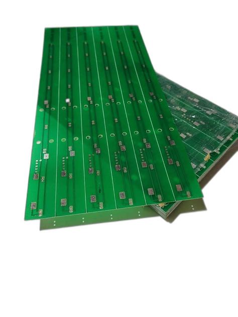
Multilayer PCB-Up To 48 Layers Manufacturing | Advanced Circuits-PcbaMake
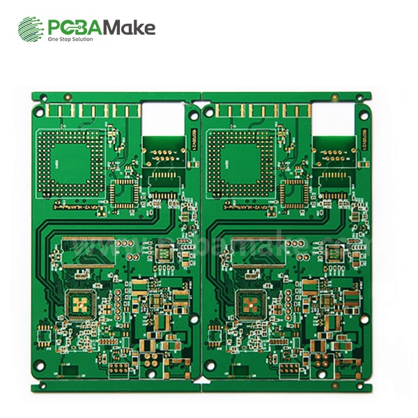 www.pcbamake.com
Multilayer PCB-Up To 48 Layers Manufacturing | Advanced Circuits-PcbaMake
Kicad Update Pcb From Schematic How Too Link An Existing Sch
 diagramudarim5oc.z21.web.core.windows.net
Kicad Update Pcb From Schematic How Too Link An Existing Sch
DIY A Card Wallet That Even Beginners Can Make Very Easy / Sewing
 www.pinterest.com
DIY A card wallet that even beginners can make very easy / sewing ...
PCB Designing - How To Design A PCB (Step By Step) | PDF | Printed
 www.scribd.com
PCB Designing - How To Design A PCB (Step by Step) | PDF | Printed ...
How To 3D Print A Model Of Your PCB | Step By Step
 www.fedevel.com
How To 3D Print a Model of Your PCB | Step by Step
Top 10 Best And Free PCB Layout Design Software In 2023 - IBE Electronics
 www.pcbaaa.com
Top 10 best and free PCB layout design software in 2023 - IBE Electronics
PCB Soldering Techniques & Best Practices For Absolute Beginners
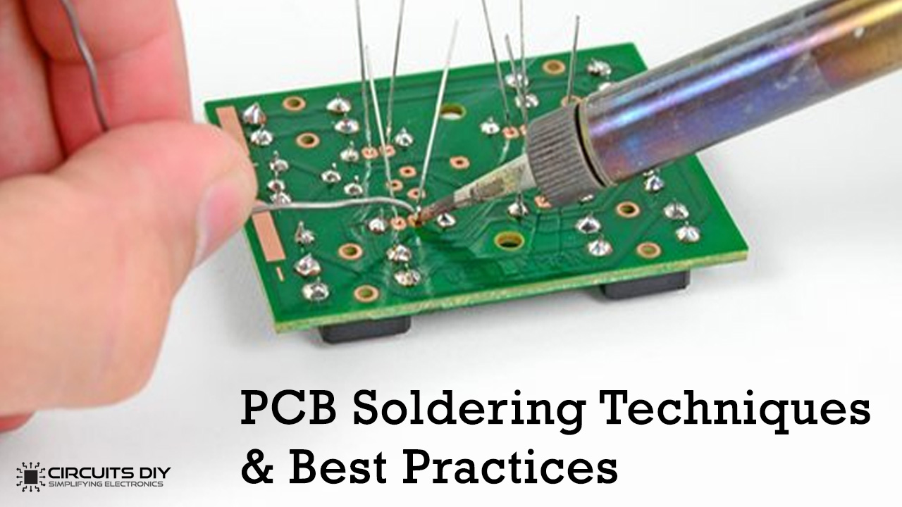 circuits-diy.com
PCB Soldering Techniques & Best Practices For Absolute Beginners
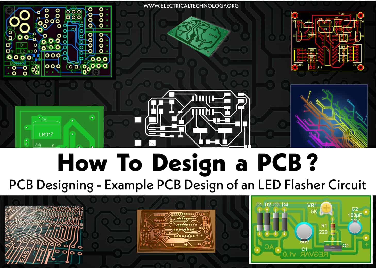
Pcb Designing How To Design A Pcb Step By Step Guide – Artofit
 www.artofit.org
Pcb designing how to design a pcb step by step guide – Artofit
Pcb Designing How To Design A Pcb Step By Step – Artofit
 www.artofit.org
Pcb designing how to design a pcb step by step – Artofit
How To Etch A PCB ? Step By Step - Artist 3D
 artist-3d.com
How to Etch a PCB ? Step by Step - Artist 3D
PCB Silkscreen | PCB Legend | Circuit Board Marking
 www.wellpcb.com
PCB Silkscreen | PCB Legend | Circuit Board Marking
Pcb Designing How To Design A Pcb Step By Step – Artofit
 www.artofit.org
Pcb designing how to design a pcb step by step – Artofit
Pcb Designing How To Design A Pcb Step By Step – Artofit
 www.artofit.org
Pcb designing how to design a pcb step by step – Artofit
18 Easiest Baking Recipes That Even Beginners Can Make – Artofit
 www.artofit.org
18 easiest baking recipes that even beginners can make – Artofit
How Do I Convert A Schematic To PCB Layout In KiCad (Step By Step) - RayPCB
 www.raypcb.com
How do I convert a Schematic to PCB Layout in KiCad (Step By Step) - RayPCB
Pcb Designing How To Design A Pcb Step By Step – Artofit
 www.artofit.org
Pcb designing how to design a pcb step by step – Artofit
Pcb Designing How To Design A Pcb Step By Step – Artofit
 www.artofit.org
Pcb designing how to design a pcb step by step – Artofit
Schematic To Pcb Converter How To Convert Schematic Pcb Layo
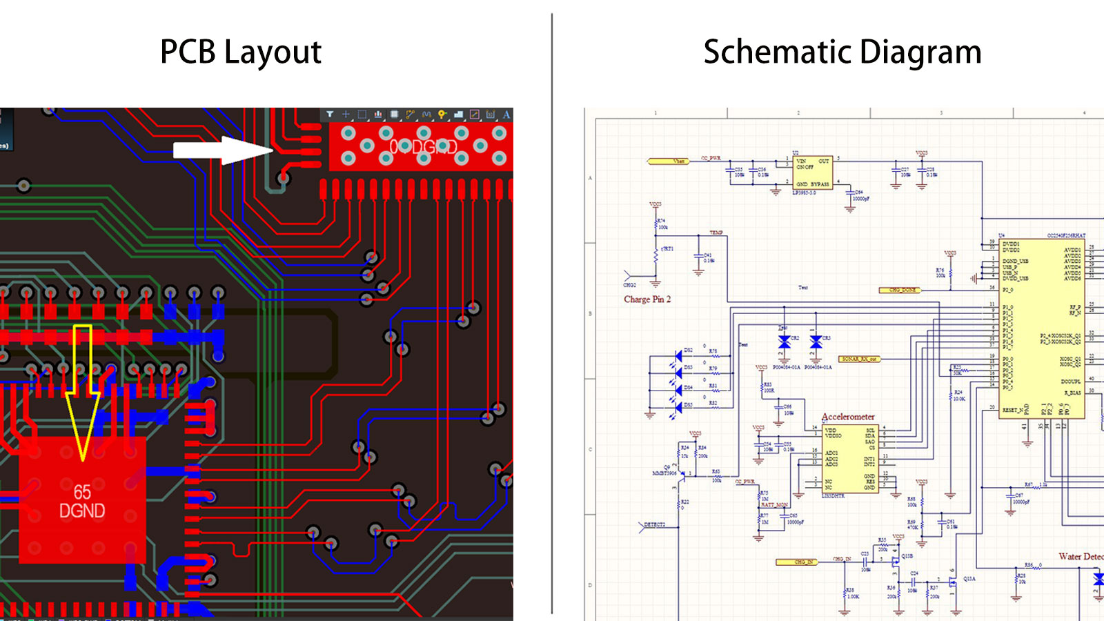 lilidu73hdrcircuit.z21.web.core.windows.net
Schematic To Pcb Converter How To Convert Schematic Pcb Layo
PCB Design Process
 mungfali.com
PCB Design Process
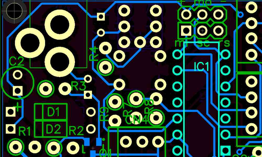
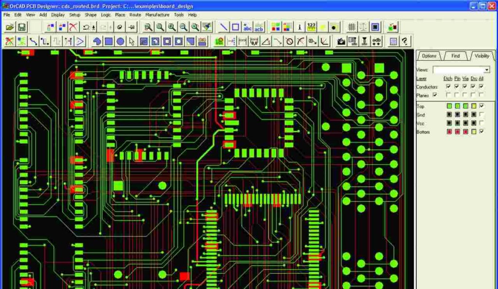
How To Convert PCB To Schematic Diagram? - RayPCB
 www.raypcb.com
How to Convert PCB to Schematic Diagram? - RayPCB
Pcb Designing How To Design A Pcb Step By Step – Artofit
 www.artofit.org
Pcb designing how to design a pcb step by step – Artofit
The Best Skincare Routine For Men – Even Beginners Can Follow
 lifeandtrendz.com
The Best Skincare Routine For Men – Even Beginners Can Follow ...
Pcb soldering techniques & best practices for absolute beginners. How to build a detailed bom (bill of materials) for pcb manufacturing .... Your guide to pcb design basics & steps